

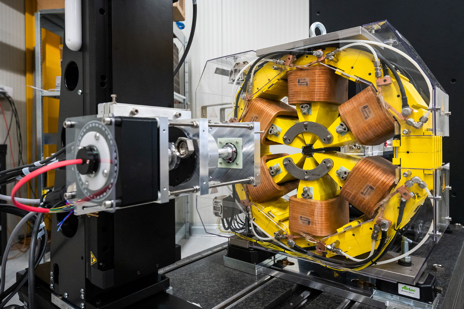
The future of electronics will depend on more than simply making components smaller. It will also rely on our ability to engineer materials in which light and electrical charges can be precisely controlled, minimizing energy losses and power consumption. Achieving this requires a junction: a region where two distinct electronic environments meet, enabling the separation of charges generated by light.
An international research team investigated molybdenum disulfide (MoS₂), a two-dimensional semiconductor consisting of atomically thin layers. The approach is particularly elegant: rather than combining different materials, which can introduce defects at their interface, the researchers created two distinct electronic regions within a single MoS₂ sheet. The crystal lattice remains continuous, while the electronic landscape through which electrons move is modified.
Part of the material is placed in contact with an insulating substrate, chromium oxychloride. This interaction induces a small charge transfer, making the affected region less electron-rich than before. The result is a lateral n⁺–n⁻ homojunction: a single material with two distinct electronic environments, separated by a boundary that promotes directional charge separation.
At Elettra’s Spectromicroscopy beamline, micro-angle-resolved photoemission spectroscopy (micro-ARPES) provided direct experimental evidence of this change in electronic energy structure. The resulting device exhibited a photovoltaic response without an externally applied voltage, achieving an open-circuit voltage of 0.87 volts and demonstrating self-powered photodetection capabilities. This measurement represents more than a laboratory result: it marks the point at which a materials-design concept translates into experimentally observable device performance.
More news
16 October 2026 | NEWS
Advanced Accelerator Control: International Exchange at TWoAFC
8 October 2026 | NEWS
“Gilberto Vlaic” XVIII School on Synchrotron Radiation
29 September 2026 | NEWS
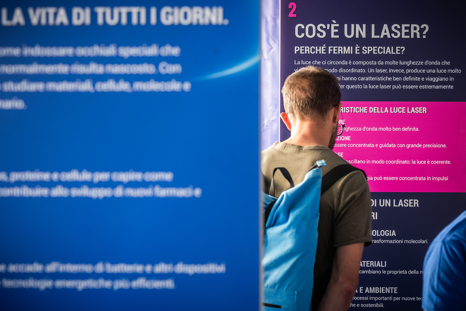
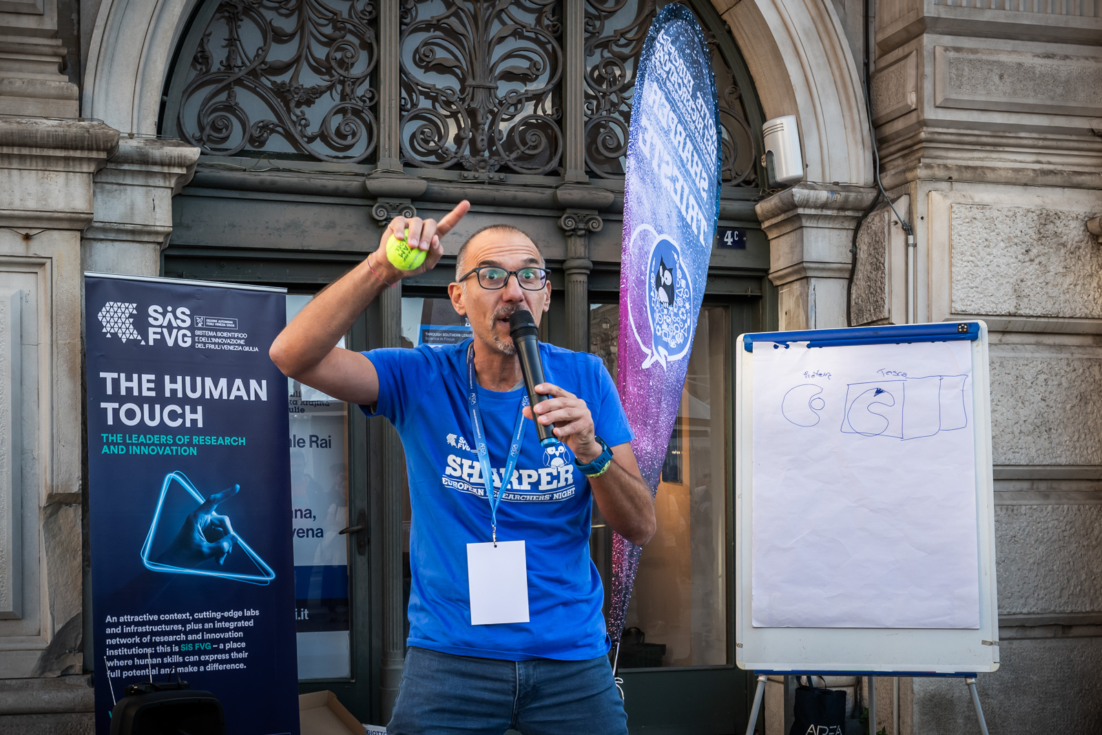
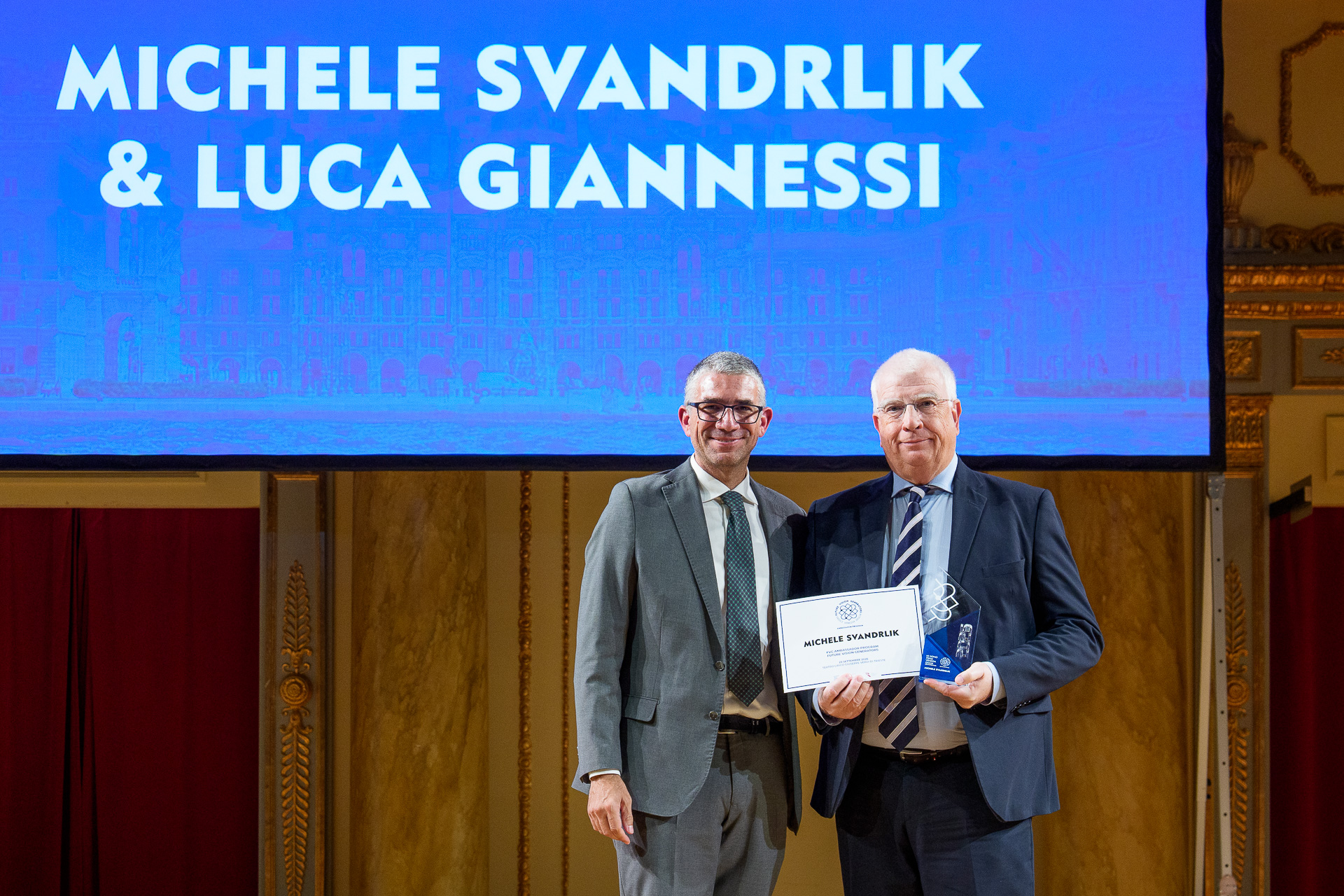
Elettra Sincrotrone Trieste at Trieste Next 2026
12 September 2026 | NEWS
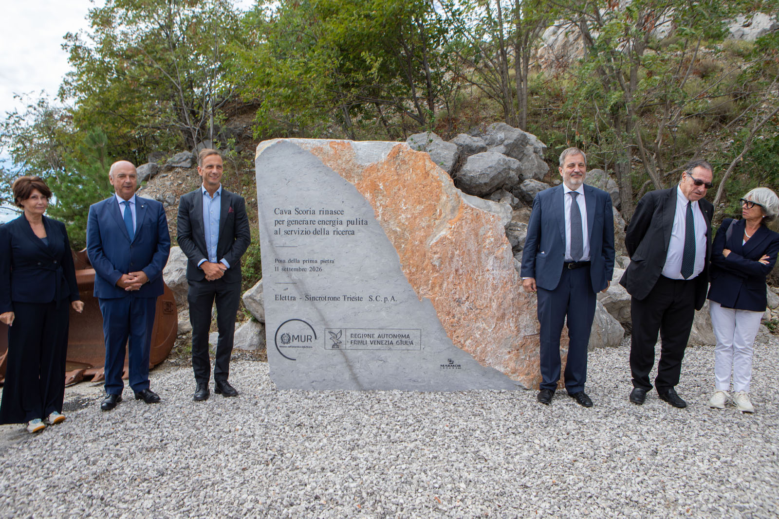
Green Energy: Elettra lays the foundation stone for its new photovoltaic park







17 November 2025 | NEWS
4th Pulsed Power Radio Frequency Sources Workshop


22 September 2025 | NEWS
GIPE25: German and Italian Physics Students at Elettra and FERMI


27 June 2025 | NEWS
Slovenian Delegation Visits Elettra Sincrotrone Trieste


29 January 2025 | NEWS